AQC has the expertise to think along and advise during the design phase of the PCB. We assure you that we will answer all questions quickly, adequately, but above all in a customer-oriented way.
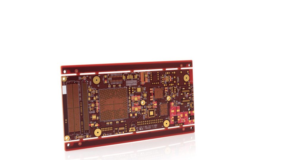
Product High Density Interconnect (HDI)
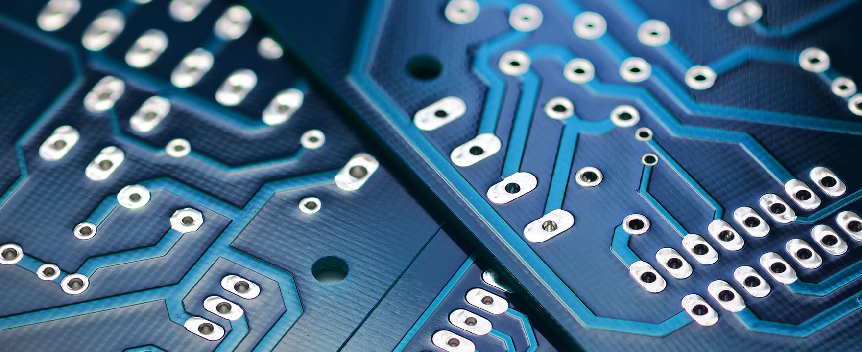
HDI is one of the fastest growing technologies in the PCB industry. It has a higher track density compared to a regular PCB. HDI boards often contain blind and/or buried via's.
Using an HDI board provides more opportunities for components to be placed on both sides of the board. HDI technology uses the non-mechanical drilling method which mainly uses LDI (laser). Also, different ways of filling and stacked holes are used during the manufacturing process.
CapabilitiesThe capabilities of High Density Interconnect (HDI)
These are extremely wide ranging in the field of HDI PCBs. AQC can advise you during your design process without any obligations. We also check if your PCB is manufacturable.
More information- Smaller in size and weight
With an HDI board, you can fit more components on both sides of the PCB. This allows you to get more functionality out of a small area. With HDI technology, you can add functionality while reducing the size and weight of your products.
- Improved electrical performance
Due to the shorter distance between components and a larger number of transistors. These characteristics reduce power consumption, this improves signal transmission.
- Increase in price/quality ratio
HDI cards can be cheaper than other options with proper planning and production because they require fewer raw materials due to their smaller size and the low number of layers they require.
- Increasing reliability
Smaller aspect ratios and the high-quality construction of microvias can increase the reliability of your PCB and your final product.
Interested? Request a quote directly
We provide excellent Advise & support
- Advice throughout the design process
- Verification that the product is manufacturable
- Tips & tricks for your PCB Design Project
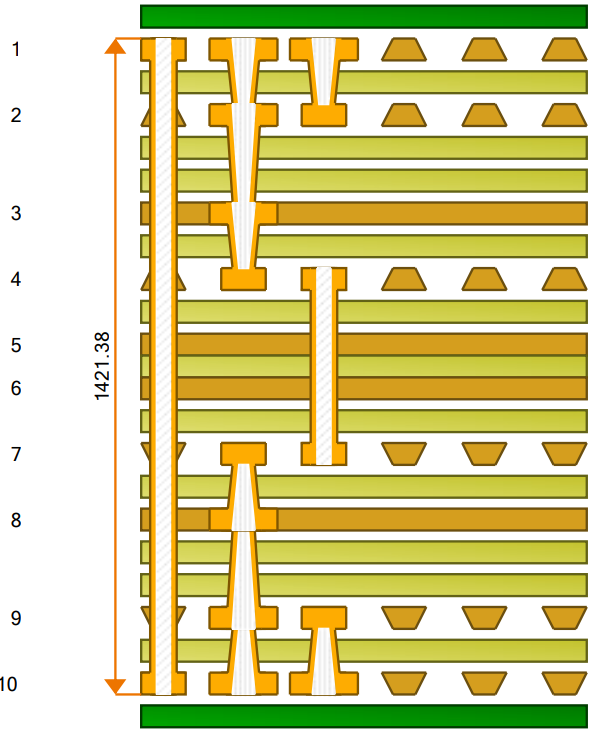
Example of a 10-layer HDI PCB
- Plated through holes
- Blind Via’s
- Stacked Via’s
- Buried via’s
4 Press cycles
- Layer 4 to 7
- Layer 3 to 8
- Layer 2 to 9
- Layer 1 to 10
ProductsDiscover products
The most ideal manufacturer for each type of product. Quality/delivery time/price/volume/reliability/technology. Please specify what is important for you.
Request a quoteCapabilitiesExplore capabilities
Not only capabilities in products but also in production locations on other continents. This allows AQC to easily switch in case of a calamity.
Explore capabilities
We treasure our Lab & quality
Explore moreWe cherish our independence, especially in quality control. Our in-house laboratory is equipped to double check the quality of delivered products. Did we receive exactly what you asked for, undamaged and ready to use? No product leaves the AQC headquarters without inspection according to AQL method.
Interested? Request a quote directly
Do you have any questions or want to make an appointment?Contact us
- info@aqcbv.com Send us an email
- 088-0045500 Reachable from 08.00 to 17.00 hours